AI4FR Virtual Shack Tour 

Hallicrafters Items


Production Year 1974 / Original cost is unknown

The Hallicrafters HC-150 is a solid state, battery operated, hand-held, Frequency Modulated(FM) transceiver. The receiver section is of the super-heterodyne, dual-conversion type, while the transmitter is crystal controlled. The transceiver was accepted back in the 1970's by the Federal Communication Commission(FCC) for narrow band FM with a deviation of around 5 KHz. The Hallicrafters company manufactured the transceiver for use in public safety, Industrial, land transportation and other domestic public radio services. The HC-150 has a total of 3 Integrated circuits. The HC-150 transceiver incorporates 11 diodes and 11 transistors in the receiver section, while the transmitter has 4 diodes and 12 transistors in its circuitry.

The frequency range of the HC-150 is between 132 MHz to 174 MHz. It is a one to six channel transceiver with the actual number of channels being a user supplied option. The loudspeaker which faces out towards the front of the unit is of the permanent magnet moving coil design. Received signals exit through a slotted section on the front of the unit. The speaker is rated at 32 ohms and has an audio output rating of 0.5 watts. The audio distortion is less then 5% at the rated output. The HC-150 has an internally threaded antenna jack located on the top of the transceiver. The operator had the choice of three antenna options. One option was a flexible whip antenna as seen on this web page, a second option was a telescoping antenna, while the third was a flexible whip antenna that was used in conjunction with the MS-402 remote microphone and speaker combination.  

On the left side of the transceiver is a Push-To-Talk(PTT) button with a monitor button/switch directly above it. The monitor button/switch has several features. When it is switched towards the front of the transceiver the Continuous Tone Controlled Squelch(CTCS) circuit is active. When the monitor button is pressed and held in, the CTCS is disabled. When it is switched towards the back of the unit, the CTCS is permanently disabled. There are three operator controls on the top of the transceiver. At the left is a channel selector knob which is not supplied with single channel models, in the middle is the squelch control which was also optional, while at the right is the On/Off and volume control knob. Also found on the top of the unit is four accessory jacks. On the left is a jack for an external speaker or earphone, next to this is a jack for an external PTT, then there is a jack for an external microphone, and at the right is the threaded antenna receptacle that requires a 50 ohm load.

The transmitter section is rated at 5 watts output and is able to produce a Frequency Modulated(FM) signal at a deviation of 5 KHz. This transceiver is supplied from the factory with a 15 volt Nickel-cadmium battery as the power source. Under normal operating conditions, the battery is expected to last up to 8 hours. The DC current drain from the battery is 14 mA with the squelch on, and 75 mA with it off. During transmit the unit draws 675 mA at 5 watts. The duty cycle of the HC-150 during transmit and receive is 5% each with the other 90% intended for standby. The HC-150 transceiver is constructed with a rugged aluminum frame and high impact plastic covers. The physical dimensions of the HC-150 is 7.5 inches high, by 2.8 inches wide, by 1.87 inches deep, and it weighs in at 34 ounces with the battery installed.

The photograph on the left is of the front and back of the HC-150 while the units are installed in the protective carrying case. The Hallicrafters name and logo are printed on the front of the carrying case. The picture on the right is of the front and back of the transceiver with the carrying case removed. The paper sticker on the back of the transceiver was placed there by a previous owner to identify the specific channels of the unit with frequencies.


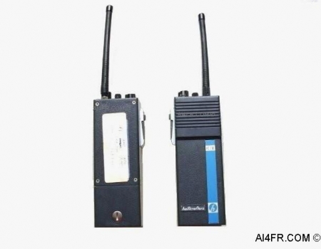
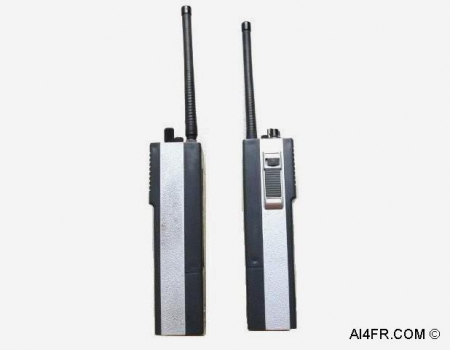
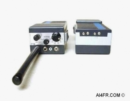
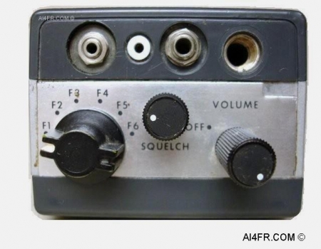
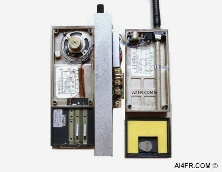
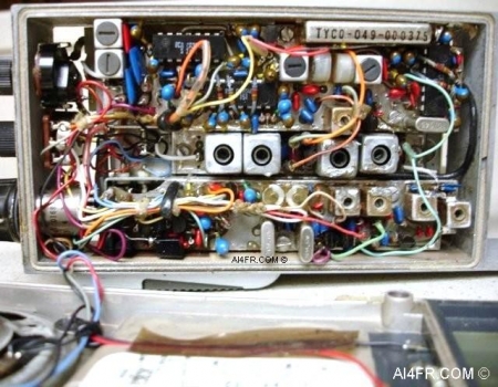
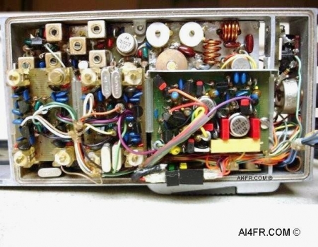
The photograph on the left is of the left and right sides of the Hallicrafters HC-150 transceiver. The picture on the right is of the top and bottom of the transceiver. Notice the tabs on the bottom of the unit which is to allow the battery to be recharged without removal.


Receive theory of operation.

To keep things simple, the theory of operation that is described below is only for the receiver circuits that are used in the two channel models. The circuits that contain additional oscillators such as numbers 3, 4, 5 and 6, which were a user requested option, operate in the same manner as oscillators number 1 and 2 in the two channel models.

When an RF signal reaches the antenna it is first routed through tuned circuits L601 and L602. At this point the signal is applied to the base of the RF amplifier transistor Q601, which has a common emitter configuration. The now amplified signal is applied to a second pair of tuned circuits, L603 and T601. At this point the local oscillators come into play. The transistor for channel 1 is Q301 and the transistor for channel 2 is Q302 which are common to the double tuned oscillator output circuit consisting of coils L301 and L302. Each local oscillator utilizes crystals in the frequency range of approximately 15.7 to 17.8 MHz. The 4th harmonic signal of the oscillators is selected in the double tuned oscillator output circuit. The signal at this point has a frequency range of around 62.7 to 71.3 MHz for the 146 to 163 MHz. Keep in mind that this is for the two channel models only.

The output signal from the double tuned oscillator circuit L302 is now applied to a frequency doubler transistor Q303. The signal at the output of Q303 has a frequency range of approximately 125.5 to 142.5 MHz and is now applied to a double tuned circuit consisting of two RF coils, L303 and L304. The RF signal from T601 is now applied to the cathode of the first mixer diode CR603. The signal output from L304 is applied to the anode of CR603 and is utilized as an injection signal. The two signals are mixed in this stage producing the first intermediate frequency of 20.5 MHz. The output signal from CR603 is amplified by the 1st IF amplifier transistor Q401, the signal is tuned with coil L401 and applied to the 20.5 MHz crystal filter FL401.

The output signal from FL401 is amplified by the 2nd IF amplifier consisting of the two transistors, Z401A and Z401B. The signal is then applied to an amplifier stage at Z401C. The 2nd conversion oscillator, transistor Z401E, is a crystal controlled oscillator operating at 20.045 MHz. The output signals from Z401C and Z401E are applied to the 2nd mixer, transistor Z401D, where the signal frequencies are mixed to produce a 455 KHz signal. The 455 KHz output signal from transistor Z401D is then filtered by a ceramic filter network having two tuned transformers, T401 and T402, and two ceramic crystals, Y402 and Y403. The output signal from the crystal filter is amplified by a four stage cascade amplifier consisting of transistors Z402A, Z402B, Z402C and Z402D. The output signal from Z402D is applied to the 1st limiter stage, containing transistors Z403A and Z403B, which removes any amplitude variations from the signal.

The output signal from the 1st limiter is then applied to the 2nd limiter stage, containing transistors Z403C and Z403D, which further removes amplitude variations not completely removed by the 1st limiter. The output signal from the 2nd limiter is applied to the discriminator transformers T403 and T404. These transformers in conjunction with diodes CR402 and CR403 convert the signal to audio. The detected audio is coupled to the audio amplifier transistor Q304, through the On/Off and volume control variable 100k ohm resistor R501. The amplified audio is applied to the audio driver transistor Q305, which provides the audio signal necessary to drive the audio output transistors. The output signal from Q305 is applied to the Push-Pull audio output amplifier consisting of transistors Q306 and Q307. The output of this stage is capacitance coupled to the speaker.

Squelch circuit.

The noise voltage used in the squelch amplifier circuitry is developed across resistor R443 and the ceramic capacitor C443, which is located in the collector circuit of transistor Z403C. This voltage is applied to the squelch amplifier transistor Q308 through the squelch control R502 which is a 5000 ohm variable resistor. The squelch detector circuit works when the output voltage from Q308 is rectified by the voltage doublers CR303 and CR304. A positive rectified voltage is developed which is proportional to the noise level(no signal). The rectified voltage is filtered by an RC network and applied to the squelch switch transistor Q309. When noise is present(no signal), this transistor is biased on. The emitter and collector voltages are DC coupled to the emitter and base respectively of the audio amplifier. When a signal is present, the squelch switch is biased off and Q304 operates normally and amplifies the audio signal.  

The photograph on the left is a close up view of the top of the transceiver. There are three operator controls on the top of the transceiver. At the left is a channel selector knob which is not supplied with single channel models, in the middle is the squelch control which was also optional, while at the right is the On/Off and volume control knob. Also found on the top of the unit is four accessory jacks. On the left is a jack for an external speaker or earphone, next to this is a jack for an external PTT, then there is a jack for an external microphone, and at the right is the threaded antenna receptacle that requires a 50 ohm load.

The picture on the right is a side view of the transceiver with the plastic case removed. The case is held together by a total of four screws. The battery compartment can be seen on the left side of the case and at the opposite end from the speaker.


The photograph on the left is of the top of the circuit board that faces towards the front of the unit. The picture on the right is of the circuit board that faces towards the back of the unit.


Transmitter theory of operation.

To keep things simple, the theory of operation that is described below is only for the transmitter circuits that are used in the two channel models. The circuits that contain additional oscillators such as numbers 3, 4, 5 and 6, which were a user requested option, operate in the same manner as oscillators number 1 and 2 in the two channel models.

The transistor for channel 1 on the schematic is Q106 and the transistor number for channel 2 is Q107. These two transistors operate as modified Colpitts oscillators utilizing crystals in the frequency range of 7.3 to 9.7 MHz. Thermistor RT101 and capacitor C125 are used for channel 1, while thermistor RT102 and capacitor C131 are used for channel 2. They form temperature compensating networks which provide the necessary frequency stability. Transistor Q102 amplifies the audio output signal from the microphone. Transistors Q103 and Q104 amplify and clip the audio output circuit from Q102 to obtain uniform modulation.

Resistor R114 adjusts the audio level supplied to the phase modulator circuit for the correct peak deviation level. The RF signal to the phase modulator which consists of diodes CR102 and CR103 is supplied by the transmitter oscillators through capacitor C129 for channel 1 and capacitor C138 for channel 2. The audio to the phase modulator is supplied by the post limiter filter network between transistor Q104 and semiconductor CR102. The output of the phase modulator is an RF signal with the phase controlled by the frequency of the audio signal driving the modulator.

The RF output signal from the phase modulator is amplified by the RF buffer amplifier transistor Q105. Then capacitor C108 couples the output signal of Q105 to the 1st tripler transistor Q201.The 1st tripler operates as a class C amplifier having a double tuned output circuit which are coils L204 and L210. These coils are tuned to the 3rd harmonic which is approximately 25 MHz of the 1st tripler input frequency. The output of the 1st tripler is then applied to the base of the 2nd tripler transistor Q202. The 2nd tripler also operates as a class C amplifier with a double tuned output circuit that consists of coils L205 and L212. These coils are tuned to the 3rd harmonic which is approximately 75 MHz of the 2nd tripler input frequency.

The signal developed at the tap of L212 drives the doubler transistor Q203. The doubler is a class C type and is tuned by the double tuned circuit of coils L206 and L213. These coils are tuned to the 2nd harmonic which is approximately 150 MHz of the doubler input frequency. The signal from Q203 is coupled to the driver transistor Q204 through coils L206 and L213 and a capacitive divider made from capacitors C219 and C220. The output signal from Q204 is coupled to the power amplifier transistor Q205, through the trifilar transformer T201. A "tee network" consisting of coils L208 and L209 along with capacitor C224 tunes the amplified transmitter output. This network provides the required selectivity at the output of the transmitter and is coupled to the antenna through a mica capacitor C225 and relay K201.


Resources:

Radios by Hallicrafters with Price Guide by Chuck Dachis

Hallicrafters owners manual  

Sam's photofacts by Howard W. Sams & Co., Inc.

      AI4FR                                                                                                                                                                                                  AI4FR                                                                                                       AI4FR

Trump WON!! Biden CHEATED!!

Avoid the experimental gene therapy C19 DEATH shot!!  

Think Critically!!

Ukraine = Corruption

Was Hitler right?

Copyright © John Whitt 2022 All rights reserved. 

Created with the QTH.com SiteBuilder.